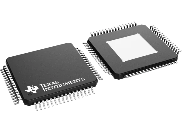
Introduction, characteristics, and applications of Texas Instruments LMK04714-Q1 dual-ring clock jitter cleaner
2/16/2024 9:40:00 AM
Summary: High-performance clock regulator with JEDEC JESD204B/C support for space applications.

The Texas Instruments LMK04714-Q1 Dual Ring Clock Jitter Cleaner is a high performance clock conditioner supporting JEDEC JESD204B/C space applications. Each of the PLL2's 14 clock outputs can be configured to drive seven JESD204B/C converters. The Texas Instruments LMK04714-Q1 can also drive other logic devices using this device and the SYSREF clock. SYSREF can be supplied using DC and AC coupling. Because the device is not limited to JESD204B/C applications, the 14 outputs can be individually configured as high-performance outputs for traditional clocking systems.
characteristic
-
AEC-Q100 Grade 1 (-40°C to 125°C)
-
3255MHz maximum clock output frequency
-
Multi-mode: dual phase locked loop, single phase locked loop, clock distribution
-
6GHz external VCO or distribution input
-
Ultra low noise, 2500MHz
-
54fs RMS jitter (12kHz to 20MHz)
-
64fs RMS jitter (100Hz to 20MHz)
-
-157.6dBc/Hz noise floor
-
3200MHz ultra-low noise
-
61fs RMS jitter (12kHz to 20MHz)
-
67fs RMS jitter (100Hz to 100MHz)
-
-156.5dBc/Hz noise floor
-
PLL2
-
The phase locked loop frequency is -230dBc/Hz
-
Phase locked loop 1/f is -128dBc/Hz
-
Phase detection rate up to 320MHz
-
Two integrated vcos: 2440MHz ~ 2600MHz and 2945MHz ~ 3255MHz
-
Up to 14 differential device clocks
-
CML, LVPECL, LCPECL, HSDS, LVDS and 2xLVCMOS programmable outputs
-
Up to 1 buffered VCXO/XO output
-
LVPECL, LVDS, 2xLVCMOS programmable
-
1-1023 CLKOUT integer division
-
1-8191 SYSREF integer division
-
25ps step analog delay SYSREF clock
-
Digital delays and dynamic digital delays for device clock and SYSREF
-
Hold mode with PLL1
-
0 delay with PLL1 or PLL2
-
High reliability
-
control baseline
-
an assembly/test site
-
1 manufacturing location
-
Extend product life cycle
-
Extended product change notifications
-
Product traceability
app
-
car radar
-
Data converter clock
-
lidar
Functional block diagram

-
Phone
+852 62639182 -
Whatsapp

