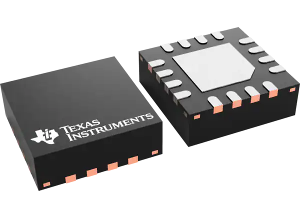
Introduction, characteristics, and applications of Texas Instruments PGA855 programmable gain instrumentation amplifier
2/16/2024 9:25:46 AM
Abstract: High-bandwidth programmable gain instrumentation amplifier with fully differential outputs.

The Texas Instruments PGA855 programmable gain instrumentation amplifier is a high-bandwidth programmable gain instrumentation amplifier with fully differential outputs. The PGA855 has eight binary gain settings, from an attenuated gain of 0.125V/V to a maximum of 16V/V, using three digital gain select pins. The output common-mode voltage can be independently set using the VOCM pin.
The Texas Instruments PGA855 architecture is optimized to drive the input of high-resolution precision analog-to-digital converters (ADCs) with sampling rates up to 1MSPS without the need for additional ADC drivers. The output stage power supply (LVSS/LVDD) is decoupled from the input stage. These devices can be connected to the ADC's power supply to protect the ADC or downstream devices from overspeed damage.
The super beta input transistors provide impressively low input bias current, delivering an extremely low input current noise density of 0.3pA/√Hz, making the PGA855 a versatile choice for virtually any sensor type. The low-noise current feedback front-end architecture provides excellent gain flatness even at high frequencies, making the PGA855 an excellent high-impedance sensor readout device. Integrated protection circuitry on the input pins handles overvoltage exceeding ±40V of the supply voltage.
characteristic
-
Eight-pin programmable binary gain
-
G (V/V) =(1/8), (1/4), (1/2), 1, 2, 4, 8 and 16
-
1ppm/°C (max) Low Gain Error Drift at G = 1V/V
-
Fully differential output
-
Separate output supply pins allow ADC input overload protection
-
Output common mode control
-
Faster signal processing
-
10MHz wide bandwidth
-
35V/µs high slew rate
-
500ns to 0.01%, 950ns to 0.0015% settling time
-
Input stage noise 7.8nV/√Hz when G = 16V/V
-
Filter options for better signal-to-noise ratio
-
External power input overvoltage protection ±40V
-
Input stage power supply range
-
Single power supply: 8V ~ 36V
-
Dual power supply: ±4V ~±18V
-
Output stage supply range
-
Single power supply: 4.5V ~ 36V
-
Dual power supply: ±2.25V ~±18V
-
Temperature range: -40℃~ +125℃
-
3mm × 3mm VQFN small package
app
-
Factory Automation and Control
-
Analog input module
-
Data Acquisition (DAQ)
-
Test and Measurement
-
Semiconductor testing
Simplify applications

-
Phone
+852 62639182 -
Whatsapp

