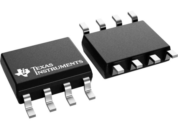
Introduction, characteristics, and applications of Texas Instruments UCC27444-Q1 4A low-side gate driver
2/22/2024 9:45:00 AM
Summary: High-speed, dual-channel, low-side gate driver that efficiently drives MOSFETs and GaN power switches.

The Texas Instruments UCC27444-Q1 4A low-side gate driver is a high-speed, dual-channel, low-side gate driver that efficiently drives MOSFETs and GaN power switches. The typical peak drive strength of UCC27444-Q1 is 4A, which reduces the rise and fall times of the power switch, improves efficiency and reduces switching losses. The device's fast propagation delay (18ns typical) yields better power stage efficiency by improving pulse width utilization, dead-band optimization, control loop response, and system transient performance.
The UCC27444-Q1 can handle -5V at its INx input, which increases the robustness of systems with moderate ground bounce. Inputs can be connected to most controller outputs for maximum control flexibility. An independent enable signal allows the power stage to be controlled independently of the main control logic. When a system fault occurs, the gate driver can be shut down quickly by pulling enable low. Many high-frequency switching power supplies exhibit noise at the gates of the power devices, which can cause driver failure and inject into the gate driver's output pins. The device's reverse voltage capability and transient reverse current enable it to withstand noise on the power device gate or pulse transformer, avoiding driver failure.
The Texas Instruments UCC27444-Q1 also features low-voltage operation and power-on-reset (POR) functionality for improved system robustness. When there is not enough bias voltage to fully boost the power device, the gate driver output is held low by the internal strong pull-down MOSFET.
characteristic
-
Suitable for automotive applications
-
AEC-Q100 qualified, the results are as follows
-
Equipment temperature level 1 (environmental operating temperature range -40℃~ +125℃)
-
Equipment HBM ESD classification level H2
-
Equipment CDM ESD classification level C6
-
Typical 4A peak source and sink drive current per channel
-
Capable of handling -5V on INA and INB input pins
-
Absolute maximum V(DD) voltage 20V
-
Wide V(DD) operating range from 4.5V to 18V
-
Two independent gate drive channels
-
Each output independently enables functionality
-
Fast propagation delay (18ns typical)
-
Fast rise and fall times (11ns and 7ns typical)
-
Typical delay match between two channels is 1ns
-
SOIC-8 and VSSOP-8 PowerPAD packaging options
-
Working junction temperature range -40℃~125℃
app
-
Switching power supply (SMPS)
-
Power factor correction (PFC) circuit
-
DC/DC converter
-
AC inverters and frequency converters
-
Microinverter
-
DC fast charging station
Functional block diagram

-
Phone
+852 62639182 -
Whatsapp

