Cart ( )
 BOM
BOMIntroduction, characteristics, and applications of Analog Devices’ ADRF5717 silicon digital attenuator
2/27/2024 9:40:00 AM
Summary: 2-bit digital attenuator, attenuation range 48dB, step 16dB.

Analog Devices' ADRF5717 silicon digital attenuator is a 2-bit digital attenuator with an attenuation range of 48dB in 16dB steps, supporting trouble-free operation. These attenuators operate over an ultra-wideband frequency range of 1MHz to 30GHz, with better than 2.8dB insertion loss and 3.3dB attenuation accuracy. The ADRF5717 silicon digital attenuator provides ATTIN and ATTOUT ports, providing RF input power handling capabilities of 30dBm steady-state average and 33dBm steady-state peak. These attenuators feature dual supply voltages of 3.3V and -3.3V and support single supply operation. The ADRF5717 silicon attenuator is compatible with complementary metal-oxide semiconductor (CMOS) and low-voltage transistor-transistor logic (LVTTL). Typical applications include industrial scanners, test and instrumentation, 5G millimeter wave cellular infrastructure, electronic countermeasures (ECM), microwave radios and very small aperture terminals (VSAT).
characteristic
-
1MHz to 30GHz ultra-wideband frequency range
-
16dB typical step to 48dB attenuation range
-
Low insertion loss:
-
1.5dB at 8GHz
-
2dB at 18GHz
-
2.8dB at 30GHz
-
Attenuation accuracy:
-
±(0.20 + 2.3% attenuation state) dB typical up to 8GHz
-
±(0.30 + 3.2% attenuation state) dB typical up to 18GHz
-
±(0.30 + 6.5% attenuation state)dB typical up to 30GHz
-
Typical step error:
-
±0.8dB typical up to 8GHz
-
±1.3dB typical up to 18GHz
-
±3.3dB typical up to 30GHz
-
High input linearity:
-
30dBm typical P0.1dB insertion loss status
-
30dBm typical P0.1dB other attenuation states
-
51dBm typical IP3 insertion loss status
-
49dBm typical IP3 other attenuation states
-
High RF power handling:
-
30dBm typical steady state average
-
33dBm typical steady-state peak value
-
Enter ATTIN and ATTOUT:
-
6.6µs typical RF amplitude settling time (final RF 0.1dB (OUT))
-
Supports single power supply operation
-
Relative phase distribution is tight
-
No low frequency spurious signals
-
Parallel mode control, compliant with ROHS standards
-
Complementary Metal Oxide Semiconductor (CMOS)/Low Voltage Transistor-Transistor Logic (LVTTL) Compatible
-
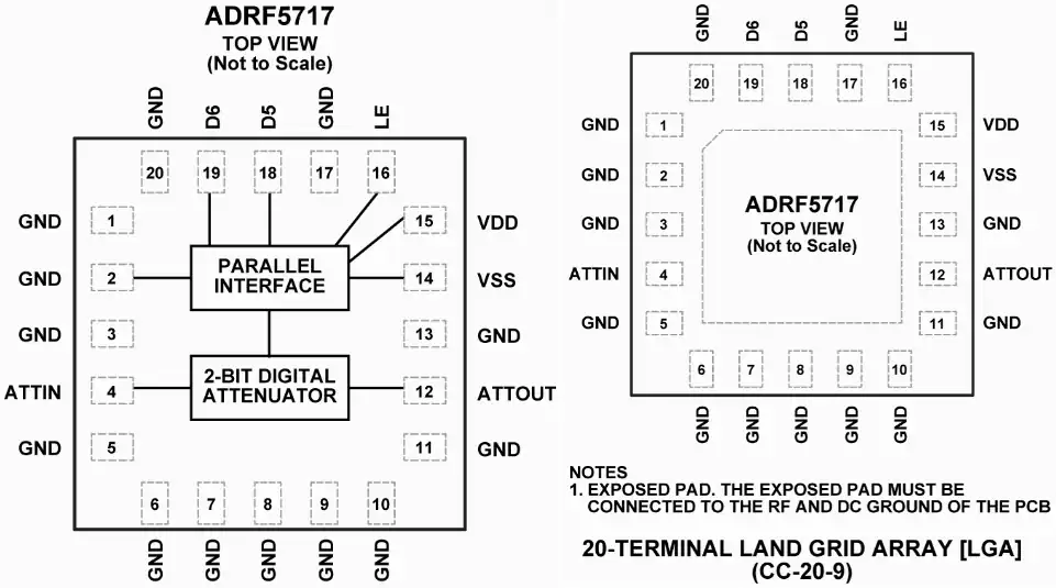
20-terminal, 3mm × 3mm, ground grid array [LGA]
app
-
Industrial scanner
-
Testing and Instrumentation
-
5G millimeter wave cellular infrastructure
-
Military radios and radars
-
Electronic Countermeasures (ECMs)
-
microwave radio
-
very small aperture terminal
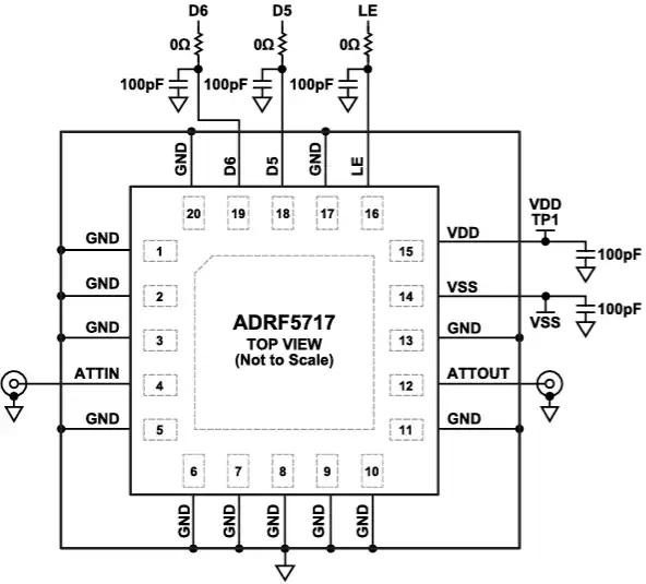
Simplified application circuit diagram
Pin configuration diagram
-
Phone
+852 62639182 -
Whatsapp