Cart ( )
 BOM
BOMIntroduction, characteristics, and applications of Texas Instruments TPS552872-Q1 fully integrated buck converter
2/12/2024 9:05:01 AM
Summary: This device is optimized to convert battery or adapter voltage to the power rails.

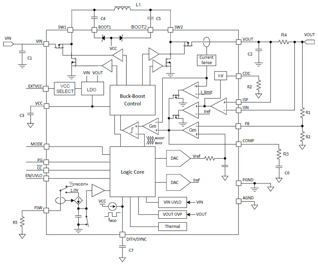
Texas Instruments TPS552872-Q1 fully integrated buck converter is optimized for converting battery or adapter voltage to the power rail. The TPS552872-Q1 integrates four MOSFET switches to provide a compact solution for a variety of applications. The TPS552872-Q1 has input voltage capability up to 36V. When operating in boost mode, the TPS552872-Q1 can output 30W from a 12V input. It is capable of delivering 25W from a 9V input voltage.
The TPS552872-Q1 uses an average current mode control scheme. The switching frequency is programmable from 200kHz to 2.2MHz with external resistors and can be synchronized to an external clock. The TPS552872-Q1 also offers optional spread spectrum to minimize peak EMI.
The TPS552872-Q1 provides output overvoltage protection, average inductor current limit, cycle-by-cycle peak current limit, and output short-circuit protection. The TPS552872-Q1 also features selectable output current limit and hiccup mode protection under sustained overload conditions to ensure safe operation.
Texas Instruments TPS552872-Q1 uses small inductors and small capacitors and has high switching frequency. It comes in a 3.0mm × 5.0mm QFN package.
characteristic
-
AEC-Q100 qualified
-
Equipment temperature level 1 (environmental operating temperature range -40℃~ +125℃)
-
Wide input and output voltage range
-
3.0V to 36V wide input voltage range
-
Programmable output voltage range from 0.8V to 22V
-
±1% reference voltage accuracy
-
Adjustable output voltage compensates for voltage drops across the cable
-
±5% accurate output current monitoring
-
High efficiency over the entire load range
-
Efficiency is 96.7% at V(IN) = 12V, V(OUT) = 20V, I(OUT) = 1.5A
-
Efficiency is 98.3% at V(IN) = 12V, V(OUT) = 12V, I(OUT) = 2A
-
Programmable PFM and FPWM modes at light load
-
Avoid frequency interference and crosstalk
-
Optional clock synchronization
-
Programmable switching frequency from 200kHz to 2.2MHz
-
EMI Mitigation
-
Optional programmable spread spectrum
-
makes no package
-
Rich protection functions
-
Output overvoltage protection
-
Output short circuit protection hiccup mode
-
Thermal shutdown protection
-
4A average inductor current limit
-
Small solution volume
-
The maximum switching frequency can reach 2.2MHz
-
3.0mm × 5.0mm HotRod QFN package
app
-
Advanced driver assistance system (ADAS)
-
Wireless charger
-
Automotive Infotainment and Clusters
-
car tail light
Functional block diagram
-
Phone
+852 62639182 -
Whatsapp