Cart ( )
 BOM
BOMIntroduction, characteristics, and applications of Texas Instruments LM74722-Q1 ideal diode controller
2/9/2024 9:40:56 AM
Summary: Drive and control external back-to-back n-channel MOSFETs to emulate an ideal diode rectifier.

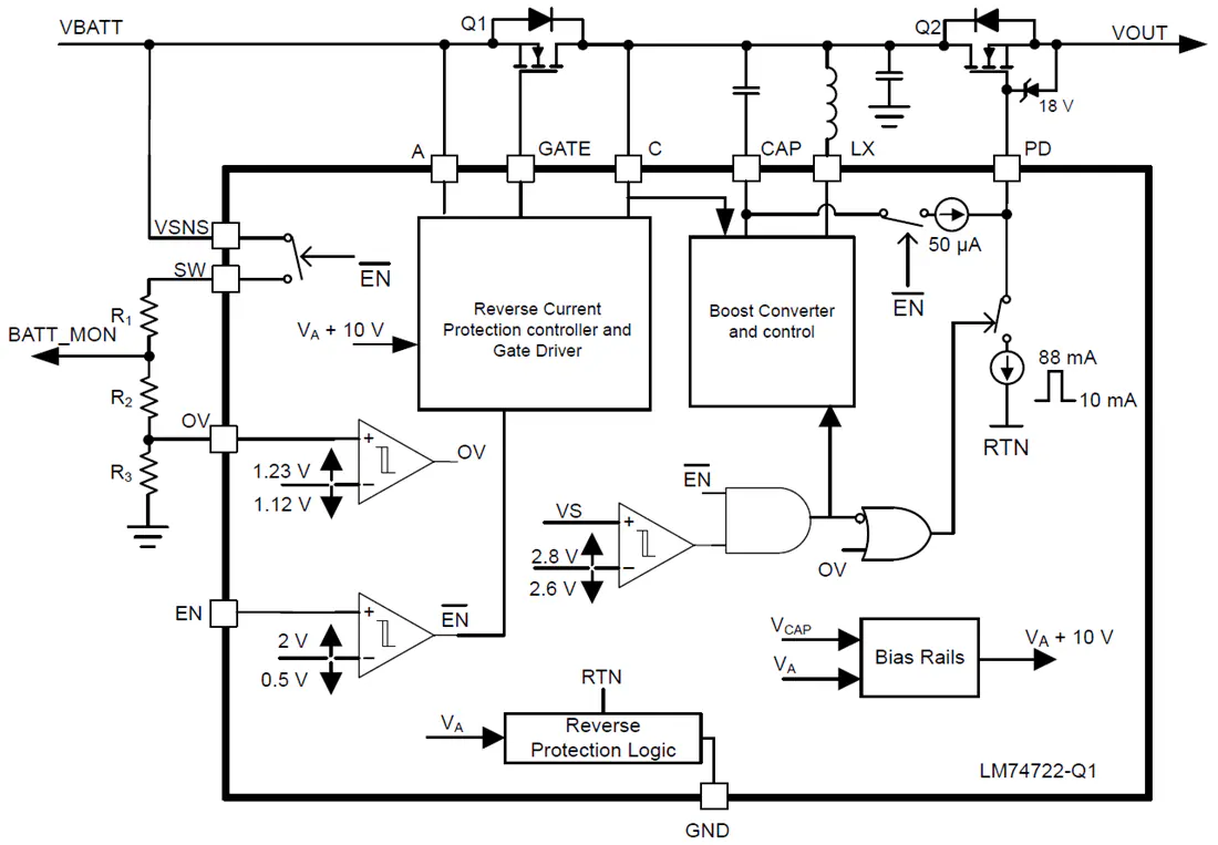
The Texas Instruments LM74722-Q1 ideal diode controller drives and controls external back-to-back n-channel mosfets to simulate an ideal diode rectifier with power path ON and OFF control and overvoltage protection. A wide input supply of 3V to 65V allows protection and control of 12V and 24V automotive battery powered ECUs. The device can protect and withstand loads with negative supply voltages as low as -65V. An integrated ideal diode controller (GATE) drives the first MOSFET to replace the Schottky diode for reverse input protection and output voltage maintenance. The powerful boost regulator with fast on and off comparators ensures robust and efficient MOSFET switching performance during automotive testing (e.g. ISO16750 or LV124) where the ECU is subject to input short interruptions and AC superimposed input signals up to 200kHz frequencies. The Texas Instruments LM74722-Q1 operates with a low quiescent current of 35 μA (max), enabling always-on system designs. With a second MOSFET in the power path, the device allows load disconnect control using the EN pin. Quiescent current is reduced to 3.3µA (max) with low EN. Using the OV pin, the device features adjustable overvoltage cutoff or overvoltage clamp protection.
characteristic
-
AEC-Q100 qualified, the results are as follows
-
Equipment temperature level 1 (environmental operating temperature range -40℃~ +125℃)
-
Equipment HBM ESD Classification Level 2
-
Device CDM ESD classification level C4B
-
3V to 65V input range
-
Reverse input protection down to -65V
-
Low quiescent current 35µA (max) during operation
-
3.3µA (max) shutdown current (EN = Low)
-
Ideal diode operation with 13mV A to C forward voltage drop regulation
-
Driving external back-to-back n-channel mosfets
-
Integrated 30mA boost regulator
-
Active rectification up to 200kHz
-
0.5µs fast response reverse current blocking
-
0.72µs fast forward GATE turn ON delay
-
Adjustable overvoltage protection
-
Meets automotive ISO7637 transient requirements with suitable TVS diodes
-
Available in space-saving 12-pin WSON package
app
-
car battery protection
-
ADAS domain controller
-
Advanced Audio Amplifier
-
The person in charge
Functional block diagram
-
Phone
+852 62639182 -
Whatsapp